- 您现在的位置:买卖IC网 > Sheet目录513 > SI7454CDP-T1-GE3 (Vishay Siliconix)MOSFET N-CH 100V 8-SOIC
New Product
Si7454CDP
Vishay Siliconix
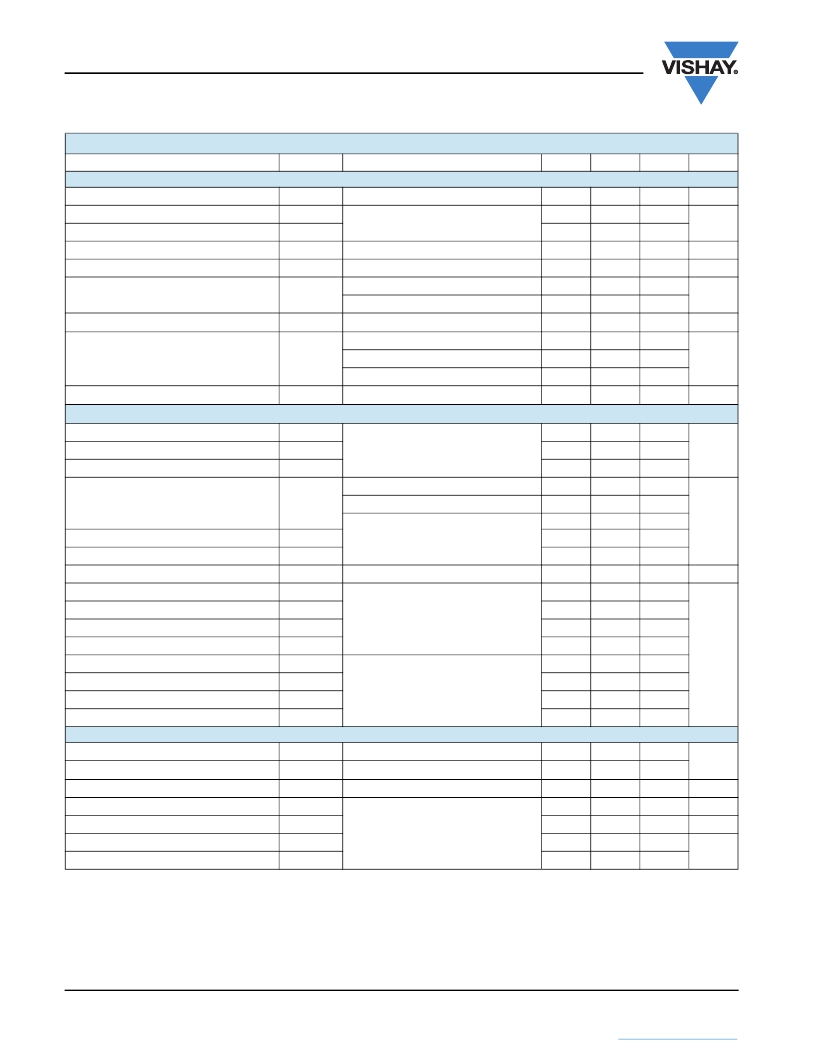
SPECIFICATIONS (T J = 25 °C, unless otherwise noted
Parameter
Symbol
Test Conditions
Min.
Typ.
Max.
Unit
Static
Drain-Source Breakdown Voltage
V DS Temperature Coefficient
V GS(th) Temperature Coefficient
V DS
? V DS /T J
? V GS(th) /T J
V GS = 0 V, I D = 250 μA
I D = 250 μA
100
47
- 5.4
V
mV/°C
Gate-Source Threshold Voltage
V GS(th)
V DS = V GS , I D = 250 μA
1.2
2.8
V
Gate-Source Leakage
Zero Gate Voltage Drain Current
On-State Drain Current a
I GSS
I DSS
I D(on)
V DS = 0 V, V GS = ± 20 V
V DS = 100 V, V GS = 0 V
V DS = 100 V, V GS = 0 V, T J = 55 °C
V DS ?? 5 V, V GS = 10 V
V GS = 10 V, I D = 10 A
20
0.0252
± 100
1
10
0.0305
nA
μA
A
Drain-Source On-State Resistance a
R DS(on)
V GS = 7.5 V, I D = 8 A
0.027
0.033
?
V GS = 4.5 V, I D = 6 A
0.0345
0.043
Forward Transconductance a
g fs
V DS = 10 V, I D = 10 A
20
S
Dynamic b
Input Capacitance
C iss
580
Output Capacitance
Reverse Transfer Capacitance
Total Gate Charge
Gate-Source Charge
Gate-Drain Charge
C oss
C rss
Q g
Q gs
Q gd
V DS = 50 V, V GS = 0 V, f = 1 MHz
V DS = 50 V, V GS = 10 V, I D = 10 A
V DS = 50 V, V GS = 7.5 V, I D = 10 A
V DS = 50 V, V GS = 4.5 V, I D = 10 A
347
24
12.8
9.8
6.3
1.8
2.9
19.5
15
9.5
pF
nC
Gate Resistance
R g
f = 1 MHz
0.8
3.8
7.6
?
Turn-On Delay Time
t d(on)
8
16
Rise Time
Turn-Off Delay Time
t r
t d(off)
V DD = 50 V, R L = 5 ?
I D ? 10 A, V GEN = 10 V, R g = 1 ?
12
16
24
32
Fall Time
Turn-On Delay Time
t f
t d(on)
10
10
20
20
ns
Rise Time
Turn-Off Delay Time
Fall Time
t r
t d(off)
t f
V DD = 50 V, R L = 5 ?
I D ? 10 A, V GEN = 7.5 V, R g = 1 ?
12
17
10
24
34
20
Drain-Source Body Diode Characteristics
Continuous Source-Drain Diode Current
Pulse Diode Forward Current a
I S
I SM
T C = 25 °C
22
40
A
Body Diode Voltage
Body Diode Reverse Recovery Time
Body Diode Reverse Recovery Charge
Reverse Recovery Fall Time
Reverse Recovery Rise Time
V SD
t rr
Q rr
t a
t b
I S = 4 A
I F = 5 A, dI/dt = 100 A/μs, T J = 25 °C
0.78
31
28
15
16
1.2
62
56
V
ns
nC
ns
Notes:
a. Pulse test; pulse width ? 300 μs, duty cycle ? 2 %.
b. Guaranteed by design, not subject to production testing.
Stresses beyond those listed under “Absolute Maximum Ratings” may cause permanent damage to the device. These are stress ratings only, and functional operation
of the device at these or any other conditions beyond those indicated in the operational sections of the specifications is not implied. Exposure to absolute maximum
rating conditions for extended periods may affect device reliability.
www.vishay.com
2
Document Number: 65940
S10-0784-Rev. A, 05-Apr-10
This document is subject to change without notice.
THE PRODUCTS DESCRIBED HEREIN AND THIS DOCUMENT ARE SUBJECT TO SPECIFIC DISCLAIMERS, SET FORTH AT www.vishay.com/doc?91000
发布紧急采购,3分钟左右您将得到回复。
相关PDF资料
SI7455DP-T1-GE3
MOSFET P-CH D-S 80V PPAK 8SOIC
SI7456DP-T1-GE3
MOSFET N-CH 100V 5.7A PPAK 8SOIC
SI7457DP-T1-GE3
MOSFET P-CH D-S 100V PPAK 8SOIC
SI7460DP-T1-GE3
MOSFET N-CH 60V 11A PPAK 8SOIC
SI7461DP-T1-GE3
MOSFET P-CH 60V 8.6A PPAK 8SOIC
SI7462DP-T1-GE3
MOSFET N-CH D-S 200V 8-SOIC
SI7465DP-T1-GE3
MOSFET P-CH 60V 3.2A PPAK 8SOIC
SI7530DP-T1-GE3
MOSFET N/P-CH 60V PWRPAK 8-SOIC
相关代理商/技术参数
SI7454DDP-T1-GE3
功能描述:MOSFET 100volt 33mOhms@10V 21A N-Ch T-FET
RoHS:否 制造商:STMicroelectronics 晶体管极性:N-Channel 汲极/源极击穿电压:650 V 闸/源击穿电压:25 V 漏极连续电流:130 A 电阻汲极/源极 RDS(导通):0.014 Ohms 配置:Single 最大工作温度: 安装风格:Through Hole 封装 / 箱体:Max247 封装:Tube
SI7454DP
制造商:VISHAY 制造商全称:Vishay Siliconix 功能描述:N-Channel 100-V (D-S) MOSFET
SI7454DP_06
制造商:VISHAY 制造商全称:Vishay Siliconix 功能描述:N-Channel 100-V (D-S) MOSFET
SI7454DP-T1
功能描述:MOSFET 100V 7.8A 4.8W RoHS:否 制造商:STMicroelectronics 晶体管极性:N-Channel 汲极/源极击穿电压:650 V 闸/源击穿电压:25 V 漏极连续电流:130 A 电阻汲极/源极 RDS(导通):0.014 Ohms 配置:Single 最大工作温度: 安装风格:Through Hole 封装 / 箱体:Max247 封装:Tube
SI7454DP-T1-E3
功能描述:MOSFET 100V 7.8A 4.8W RoHS:否 制造商:STMicroelectronics 晶体管极性:N-Channel 汲极/源极击穿电压:650 V 闸/源击穿电压:25 V 漏极连续电流:130 A 电阻汲极/源极 RDS(导通):0.014 Ohms 配置:Single 最大工作温度: 安装风格:Through Hole 封装 / 箱体:Max247 封装:Tube
SI7454DP-T1-E3
制造商:Vishay Siliconix 功能描述:MOSFET
SI7454DP-T1-GE3
功能描述:MOSFET 100V 7.8A 4.8W 34mohm @ 10V RoHS:否 制造商:STMicroelectronics 晶体管极性:N-Channel 汲极/源极击穿电压:650 V 闸/源击穿电压:25 V 漏极连续电流:130 A 电阻汲极/源极 RDS(导通):0.014 Ohms 配置:Single 最大工作温度: 安装风格:Through Hole 封装 / 箱体:Max247 封装:Tube
SI7455DP-T1-E3
功能描述:MOSFET 80V 28A 83.3W RoHS:否 制造商:STMicroelectronics 晶体管极性:N-Channel 汲极/源极击穿电压:650 V 闸/源击穿电压:25 V 漏极连续电流:130 A 电阻汲极/源极 RDS(导通):0.014 Ohms 配置:Single 最大工作温度: 安装风格:Through Hole 封装 / 箱体:Max247 封装:Tube
